
Email:
zhaizhongbing723@gmail.com
深圳市由你创科技有限公司 -- 软件行业的源头工厂


zhaizhongbing723@gmail.com


FPGA (Field programmable Logic Array) is a highly flexible hardware development platform, which can implement various applications and functions. The development process of FPGA includes a series of steps from requirement analysis to verification, which involves hardware design, software development and verification testing. The flow of FPGA development is detailed in the following.
The first step in FPGA development is requirement analysis. At this stage, the unicrom development team had to communicate with the customer to understand their needs and feature requirements. This step is very critical because it directly affects the direction of subsequent hardware design and software development.
The second step is the hardware design. In this phase, the engineer needs to design the hardware circuit of the FPGA according to the results of the requirement analysis. This includes choosing FPGA models, determining peripheral interfaces, designing logic circuits, and so on. Typically, engineers use a hardware description language, such as VHDL or Verilog, to describe how a circuit functions and is connected.
The third step is software development. In this phase, engineers need to use specialized development tools, such as XilinxISE or QuartusPrime, etc., to write and debug the configuration files of the FPGA. These configuration files include the logic design of the hardware circuit, constraint information, and so on. Engineers can perform simulation and debugging through the provided development tools to ensure the correctness and reliability of the software.
The fourth step is synthesis and mapping. In the synthesis phase, the development tool will convert the description file of the logic circuit into a form that can be understood by the FPGA. In this process, the development tool will use the resources inside the FPGA chip to map the logic circuit to the Programmable Logic Cell (PL) and Programmable Interconnection Network (PCN) of the FPGA.
The fifth step is the layout and wiring. In this phase, the development tool will plan and optimize the location and connection relationship of FPGA resources according to the requirements and constraints of the logic circuit. In particular, the locations of logic elements (gates, registers, etc.) and the connections between them are determined. This process needs to take into account the constraints of latency, power consumption, and layout.
The sixth step is to generate and download the bitstream. In this phase, the development tool generates the FPGA configuration bitstream file based on the layout and routing results. This bitstream file contains the configuration and initialization information of the FPGA. Developers can download bitstream files to the FPGA chip through the FPGA development board or JTAG interface.
The last step is validation and testing. In this phase, developers need to verify and test the designed circuit using FPGA development board and test equipment. Engineers write test code to verify the function and performance of the circuit by inputting different signals and data. The process also includes timing analysis, power testing and boundary scan.
To summarize, the detailed flow of FPGA development includes requirements analysis, hardware design, software development, synthesis and mapping, placement and routing, bitstream generation and download, and verification and testing. Each link requires developer expertise and experience to guarantee the performance and quality of the final product. Therefore, it is very important to be familiar with and master the FPGA development process, which helps to improve the development efficiency and avoid some common errors and problems. Youchuang has rich application and practice in 3D simulation, artificial intelligence, big data, blockchain, Internet of things, FPGA, machine automation, machine vision, path planning and other advanced technologies. At present, it has served more than 100 types of institutions such as scientific research institutions, colleges and universities, government, enterprises and institutions, listed companies, commercial institutions and start-ups. In the future, we will continue to give full play to our unique advantages, adhere to the development concept of truth-seeking, pragmatic, open cooperation, and strive to become the “source factory” of the world first-class software industry.

Microscope Chromosome Karyotype Analysis Upper Computer Software Development
With the continuous development of biotechnological sci […]

Development of host computer program for electric servo test
The application of electric actuators in various fields […]

Development of an Intelligent Picking System for Robotic Arms Based on Machine Vision
Intelligent manufacturing is gradually becoming an impo […]

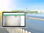
Custom Development of an Online Monitoring System for Production Equipment
The manufacturing sector plays an increasingly vital ro […]

Development of a Frequency Converter Upper Computer System
Frequency converters, as pivotal equipment for regulati […]

Custom Development of Ultrasonic Radar Testing Upper Computer
The demand for ultrasonic radars in fields such as auto […]
Software Development for Water Quality Algae Monitoring and Identification System.
Project BackgroundFaced with the professional detection […]

Smart Home Living Kitchen System: Dual-End Cooking Robot APP Development
Project Background To enhance the core competitiveness […]

Smart Weeding Machine Android and iOS Mobile Dual-Platform Control APP Program Development and Customization
Case Background With the advancement of technology and […]
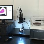
Development of an Automated Control Host Computer System for Laboratory Microscopes
Project Background A certain biotechnology company spec […]

The development of an intelligent self-service charging station control system for new energy electric vehicles
Project Background With the development of smart grids, […]

Cross-border e-commerce shop agent declaration platform system: Oudai independent declaration software customization development
Case Background According to the new regulations on com […]


WhatsApp:
Email:zhaizhongbing723@gmail.com
Address:Zone E, 10th Floor, HongKong Shenzhen International Center, Longhua District, Shenzhen
©2024 unicrom. All rights reserved.

